FPGA: Getting Us Closer To Hardware
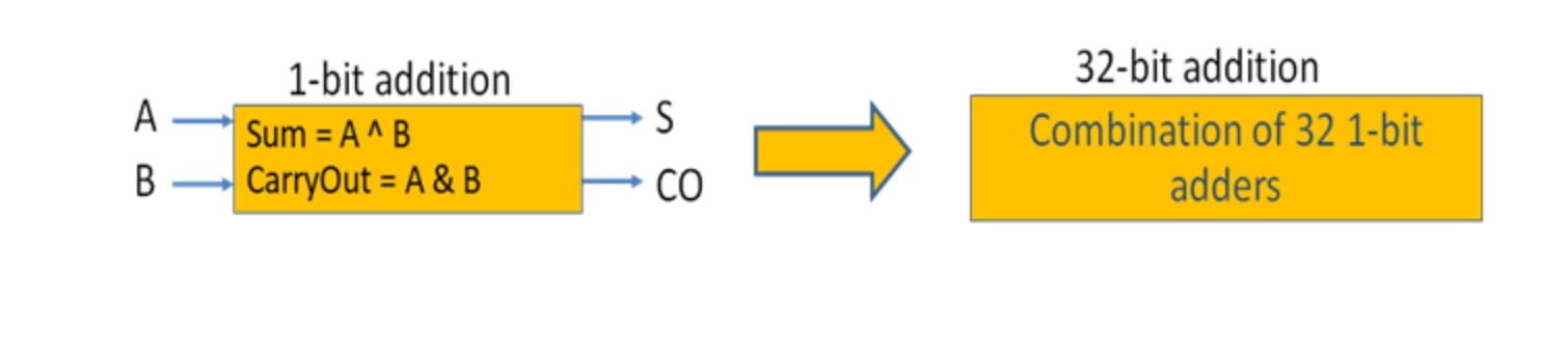
Before we get into the details of what FPGAs are, we would like to discuss what is the fastest way of achieving any computation. For example, a 1-but full-adder!
What is the fastest way to compute?
How will an addition work in a CPU?
The assembly instruction "ADD $R1, $R2, $R3" is a basic arithmetic operation commonly found in assembly language programming. Here's a breakdown of what this instruction does:
ADD: This mnemonic represents the operation being performed, which is addition in this case.
$R1, $R2, $R3: These are registers used for the operation. Registers are small, fast storage locations within the CPU used to hold data temporarily during program execution. In this instruction:
$R2 and $R3 are the source registers, containing the values to be added.
$R1 is the destination register, where the result of the addition will be stored.
So, when the "ADD $R1, $R2, $R3" instruction is executed, the contents of $R2 and $R3 are added together, and the result is stored in $R1.
In terms of hardware implementation, dedicated hardware components within the CPU, such as the arithmetic logic unit (ALU), are responsible for executing arithmetic operations like addition. The CPU decodes the assembly instruction and triggers the appropriate hardware components to perform the addition operation, fetching the values from the specified registers and storing the result back into the destination register. This process occurs at the hardware level, with electrical signals and logic gates orchestrating the operation.
Custom hardware solutions, particularly in the context of building a custom adder for specific applications, can provide the fastest implementation. Let's address each point:
ALU and Adder Operations: Both CPUs and GPUs utilize Arithmetic Logic Units (ALUs) to perform arithmetic operations, including addition. An adder is a fundamental component of an ALU responsible for adding two numbers.
Custom Hardware for Fastest Adder: Custom hardware designs can indeed provide the fastest adders tailored to specific application requirements. By optimizing the adder architecture and utilizing specialized techniques, it's possible to achieve high-speed and efficient addition operations.
Cost Considerations: Building custom hardware solutions, especially for highly optimized components like adders, can be prohibitively expensive. The design, fabrication, and testing of custom integrated circuits involve significant costs, often running into millions of dollars.
Single Application Specificity: Custom hardware solutions are typically designed for a specific application or set of tasks. Once built, they are optimized to perform those tasks efficiently. However, they lack the flexibility to adapt to different computations or applications without significant redesign and reimplementation.
Flexibility and Adaptability: One drawback of custom hardware solutions is their lack of flexibility and adaptability to handle different computations or tasks. If the application requirements change or new computations need to be performed, it may be necessary to redesign and rebuild the custom hardware, which can be time-consuming and costly.
To address the issue of flexibility and adaptability, some potential solutions include:
- Reconfigurable Hardware: Use of reconfigurable hardware platforms like FPGAs allows for flexibility and adaptability in performing various computations. FPGAs can be reprogrammed to implement different algorithms or functionalities, providing versatility in application deployment.
- General-Purpose Processors: Utilize general-purpose processors like CPUs or GPUs for tasks that require flexibility and support for diverse computations. While they may not offer the same level of performance as custom hardware for specific applications, they provide the versatility to handle a wide range of tasks.
- Hybrid Approaches: Employ hybrid computing architectures that combine custom hardware accelerators with general-purpose processors. This approach leverages the strengths of both custom hardware for specialized computations and general-purpose processors for flexibility and adaptability.
Overall, while custom hardware solutions can offer the fastest performance for specific applications, it's important to consider the trade-offs in cost, adaptability, and flexibility when evaluating their suitability for different computing tasks.
Introduction to FPGA
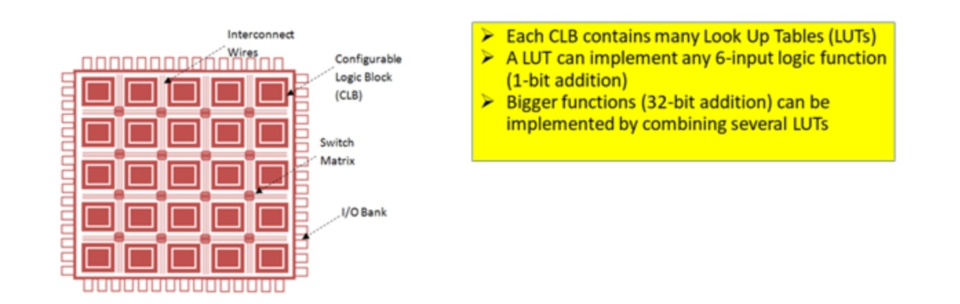
FPGA (Field-Programmable Gate Array) is indeed a configurable integrated circuit that consists of a massive array of configurable logic blocks (CLBs). Here's a further explanation:
Massive Array: FPGAs contain a large number of configurable logic blocks arranged in a grid-like structure. This array can consist of millions of these logic blocks, providing extensive resources for implementing various digital circuits and designs.
Configurable Logic Blocks (CLBs): CLBs are the fundamental building blocks of FPGAs. Each CLB typically contains a combination of logic elements, such as look-up tables (LUTs), flip-flops, multiplexers, and other programmable components. These components can be interconnected and configured to implement custom logic functions and circuits.
FPGAs offer significant flexibility and reconfigurability compared to traditional ASICs (Application-Specific Integrated Circuits) because their logic and interconnections can be programmed and reprogrammed by the user after manufacturing. This allows for rapid prototyping, iteration, and customization of digital designs without the need for costly and time-consuming custom chip fabrication.
The configurable nature of FPGAs makes them well-suited for a wide range of applications, including digital signal processing, telecommunications, embedded systems, robotics, and more. Developers can leverage FPGAs to implement custom hardware accelerators, specialized processing units, or complex control logic tailored to specific application requirements.
Re-configurability: FPGAs are indeed re-configurable, allowing users to change their functionality even after manufacturing. This flexibility is a significant advantage, as it enables rapid prototyping, testing, and iteration of digital designs without the need for costly custom chip fabrication.
Cost and Speed Trade-off: FPGAs are typically much cheaper than custom hardware designed for specific applications. While they may not offer the same level of performance as dedicated ASICs (Application-Specific Integrated Circuits), they provide a cost-effective solution for many applications. Additionally, the trade-off in speed is often acceptable given the benefits of re-configurability and rapid development.
Availability on Cloud Platforms: FPGAs are indeed available on major cloud platforms such as Amazon Web Services (AWS), Microsoft Azure, Alibaba Cloud, and others. Cloud-based FPGA instances provide users with on-demand access to FPGA resources, allowing them to deploy and scale FPGA-accelerated applications without the need for upfront hardware investment or infrastructure management.
Overall, FPGAs offer a compelling combination of re-configurability, cost-effectiveness, and availability, making them an attractive choice for a wide range of applications, including digital signal processing, machine learning, high-performance computing, and more. Their presence on cloud platforms further enhances accessibility and usability, enabling developers and organizations to leverage FPGA technology for accelerated innovation and deployment.
Let's look at how FPGAs allow exploration of implementation choices for even a very basic operation like ADDER.
Implementation Choices on an FPGA
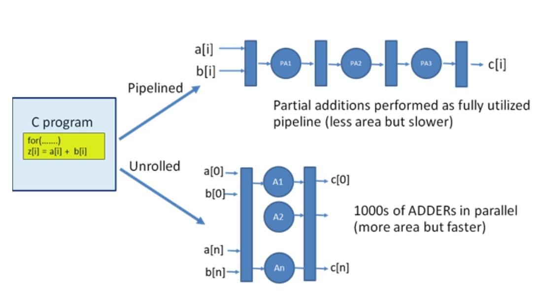
Indeed, FPGAs offer the flexibility to explore trade-offs between area (resource utilization) and speed (performance) when designing digital circuits. Here's a bit more detail on each of your points:
Flexibility for Area/Speed Trade-offs: FPGAs allow designers to optimize their designs based on specific requirements. By adjusting the configuration of logic blocks, routing resources, and other parameters, designers can explore trade-offs between area (how efficiently resources are used) and speed (how fast the circuit operates). This flexibility enables designers to tailor their designs to meet various constraints, such as power consumption, cost, and performance.
Hardware Design Skills Requirement: Designing for FPGAs does indeed require some level of hardware design skills. While modern design tools provide high-level abstractions and automation features, understanding digital logic concepts, hardware description languages (HDLs) like Verilog or VHDL, and FPGA architectures is essential for efficient and effective FPGA design. Additionally, optimizing designs for performance, resource utilization, and reliability often requires expertise in hardware design principles and methodologies.
CPU <-> FPGA Interaction: Interaction between CPUs and FPGAs can be achieved through various interfaces and protocols, depending on the application requirements. Some common methods for CPU-FPGA communication include:
- Memory-mapped I/O: FPGAs can be connected to a CPU via memory-mapped I/O interfaces, allowing the CPU to read from and write to FPGA registers or memory locations as if they were ordinary memory addresses.
- Direct Memory Access (DMA): DMA controllers can be used to transfer data between the CPU's memory and FPGA memory without CPU intervention, enabling high-speed data transfers between the two devices.
- Custom Communication Protocols: Designers can implement custom communication protocols using dedicated interfaces such as UART, SPI, I2C, or Ethernet to enable communication between CPUs and FPGAs.
- Accelerator Interfaces: FPGAs can be used as accelerators or co-processors alongside CPUs to offload compute-intensive tasks. Communication between the CPU and FPGA occurs through dedicated interfaces, with the CPU orchestrating task execution on the FPGA and exchanging data as needed.
- PCIe (Peripheral Component Interconnect Express): FPGAs can be connected to CPUs via PCIe interfaces, allowing for high-speed data transfer and communication between the CPU and FPGA over the PCIe bus.
Overall, the interaction between CPUs and FPGAs enables the creation of heterogeneous computing systems that leverage the strengths of both devices to address a wide range of computational challenges, from real-time signal processing to high-performance computing and beyond.
CPU <-> FPGA (How FPGAs work together with CPUs)
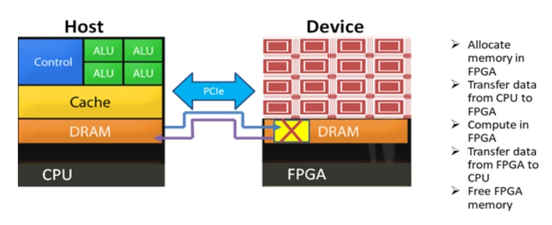
The steps for CPU-FPGA interaction are conceptually similar to those for CPU-GPU interaction, but there are differences in the technologies and frameworks used. Here's a comparison:
Setup and Configuration:
For CPU-GPU interaction, developers typically use libraries like NVIDIA's CUDA or AMD's ROCm to manage interaction between the CPU and GPU.
For CPU-FPGA interaction, developers often utilize frameworks like Intel's OpenCL (Open Computing Language) or HLS (High-Level Synthesis) tools to interface with the FPGA.
Programming Model:
CUDA provides a programming model specifically designed for NVIDIA GPUs, allowing developers to write parallel code using CUDA kernels.
OpenCL is a cross-platform framework that provides a programming model for heterogeneous computing, enabling developers to write code that can execute on CPUs, GPUs, and FPGAs. OpenCL kernels can be compiled and executed on FPGAs using tools provided by FPGA vendors.
Data Transfer:
In CPU-GPU interaction, data transfer between the CPU and GPU typically involves copying data between CPU and GPU memory using APIs provided by CUDA or similar libraries.
In CPU-FPGA interaction, data transfer between the CPU and FPGA can be managed using memory-mapped I/O, DMA (Direct Memory Access), or custom communication protocols, depending on the application requirements and hardware configuration.
Resource Management:
CUDA provides APIs for managing GPU resources, such as allocating and deallocating memory on the GPU and launching kernel functions.
OpenCL offers similar functionality for managing resources across different types of compute devices, including CPUs, GPUs, and FPGAs. Developers can use OpenCL APIs to create and manage compute contexts, memory buffers, command queues, and execute kernels on FPGA devices.
Programming Language Support:
CUDA primarily supports programming in C/C++ with extensions for parallel programming.
OpenCL supports programming in C/C++ as well as other languages like Python, and it offers a standard API for heterogeneous computing across different platforms and devices.
In summary, while the steps for CPU-FPGA interaction share similarities with CPU-GPU interaction, the technologies and frameworks used are different. OpenCL is commonly used for managing interaction with FPGAs, providing a standardized approach for heterogeneous computing across various types of compute devices.