Development of Chat-GPT-like Assistants for Chip Design Automation Clients
Background
Our client, an EDA provider, sought to enhance the accessibility and adoption of their toolsets, recognizing that designers were hesitant to embrace new tools due to the overwhelming task of digesting extensive documentation.
Challenge
Current adoption methods—such as seminars, training sessions, or reliance on a handful of experts—are time-intensive and unwieldy. A solution was needed to swiftly furnish chip designers with the requisite information, enabling independent tool usage. This necessitates employing modern techniques to address the learning curve associated with tool adoption.
Solution
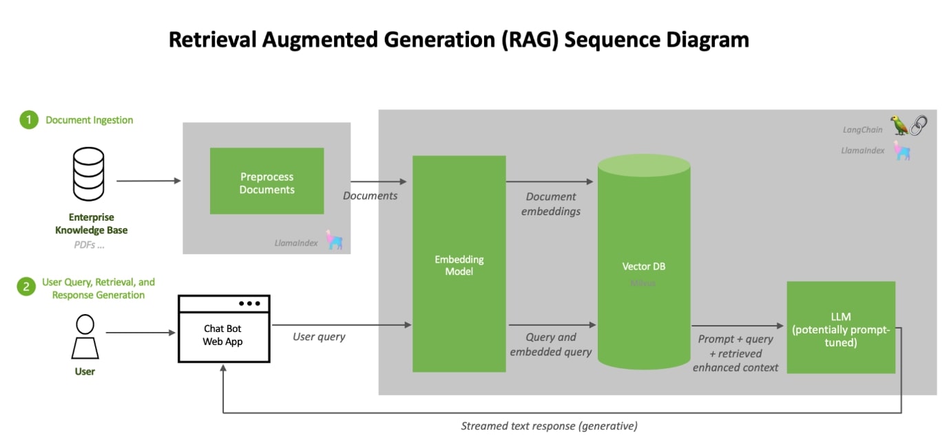
To address this, we developed a Chat-GPT-like chatbot leveraging an open-source Large Language Model (LLM) and employed the Retrieval Augmented Generation (RAG) technique to iteratively train the chosen LLM with EDA tool documentation. Integrated into the EDA tools' user interface, this system significantly expedited adoption times (from weeks to days) and boosted productivity for chip designers.
We explored three approaches: retraining the model with user documentation, training the model in Q&A format, and leveraging RAG techniques. While the first two methods offer higher accuracy, they entail greater time and expense. Conversely, the RAG technique yields reasonable accuracy with rapid turnaround.

Result
Employing the RAG framework, we successfully trained the LLM with six additional user documents for six distinct EDA tools. Additionally, we conducted prompt engineering to orient the LLM toward semiconductor knowledge. Consequently, users could obtain quick answers to tool-related queries within 2-10 seconds. Expert evaluation revealed an initial accuracy of approximately 70%, which could be further improved to 80% through question reformulation.
The implemented solution significantly enhanced user adoption of new tools. Previously, onboarding a new user took 4-5 weeks, but with our solution, this time was slashed to 3-4 days.
Impact
Our client was able to onboard ten times more users than before, resulting in cost savings for both the EDA company and chip design houses. Consequently, both tool creators and chip design houses observed increased productivity and reduced costs.
